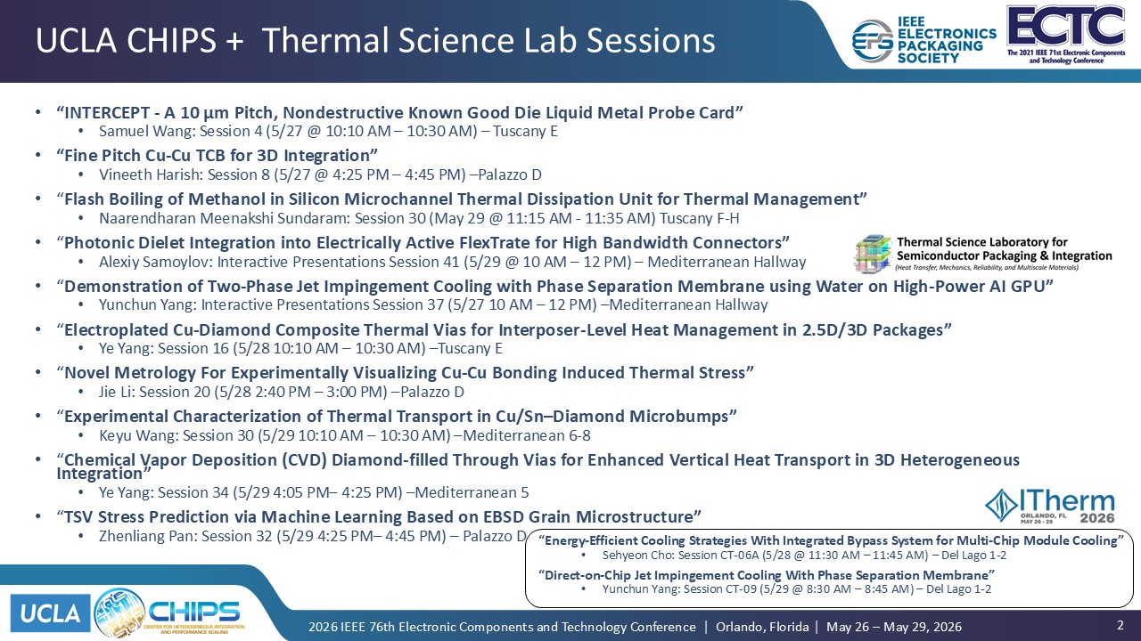
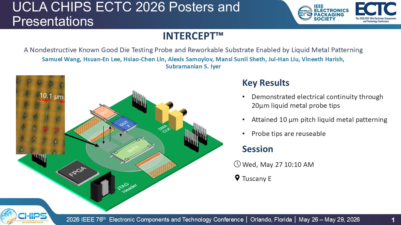
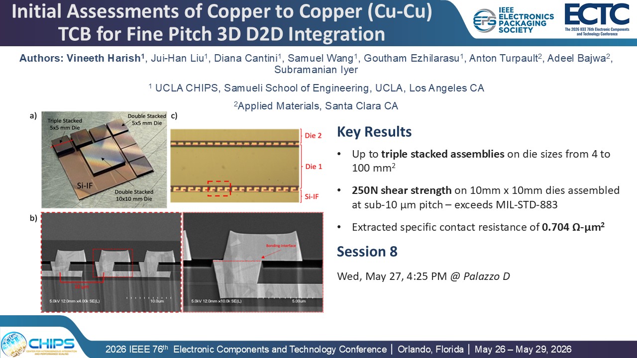
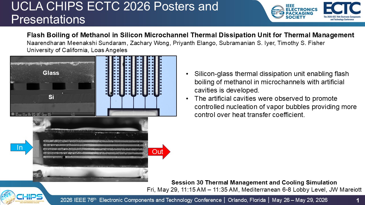
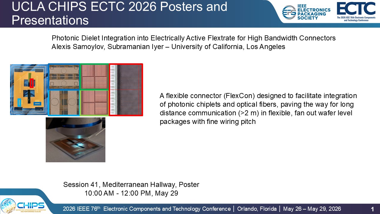
Interpret and implement Moore’s Law to include all aspects of heterogeneous systems and develop architectures, methodologies, designs, components, materials and manufacturable integration schemes, that will shrink system footprint and improve power and performance.
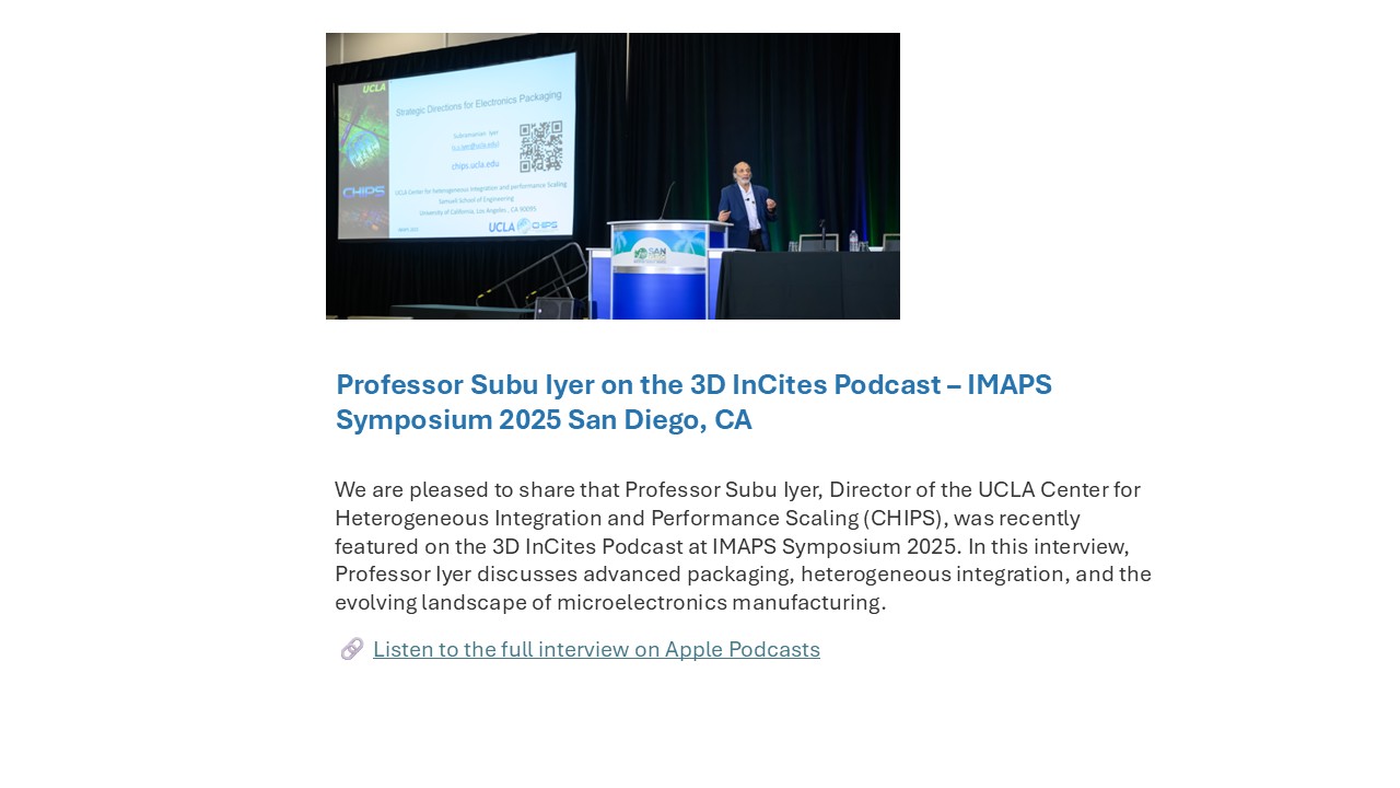
UCLA CHIPS Director Prof. Subramanian Iyer discusses the growing role of advanced chip packaging in enabling next-generation AI systems. The feature highlights why packaging technologies have become essential to semiconductor innovation and global competitiveness, and the importance of continued research in this rapidly evolving field.
Recent data indicates a soft decline in engineering Ph.D. enrollment, signaling potential risks to the long-term research talent pipeline. While not yet critical, factors such as funding uncertainty, visa challenges, and global competition are contributing to this trend. This presents a strategic inflection point—reinforcing the need for stronger industry partnerships,...
UCLA
UCLA Luskin Conference Center
Virtual Event
Virtual
Hello, I am Joseph Camyre, the Webmaster for CHIPS Lab! If you run into any issues with the website, please don't hesitate to send me an email at jcamyre127@g.ucla.edu!